Cmos Diagram For Half Adder Circuit : Half Adder Circuit Theory And Working Truth Table Schematic Realization
Draw the stick diagram of half adder circuit; Half adder is a combinational arithmetic circuit that adds two numbers and produces a sum bit (s) and carry bit (c) as the output. Gates implementation of half adder. If a and b are the input bits . Half adder is a combinational circuit that performs simple addition of two single bit.

This results in low input capacitance and high speed operation.
Though the implementation of larger logic diagrams is possible with the above full adder logic a simpler symbol is mostly used to represent the operation. This results in low input capacitance and high speed operation. Appropriate device sizing can result in equal and symmetrical drive current which leads to a sunstainable design. Draw the stick diagram of half adder circuit; In this video, i have explained cmos half adder with following timecodes: Fig.3 schematic diagram of existing half adder using static cmos technique. Fa = full adder, ha = half adder. The block diagram of a half adder is shown below. The circuit diagram of simplified half adder is shown in fig.6. The output is the sum of the two bits (s) and the carry (c). Half adder is a combinational circuit that performs simple addition of two single bit. Digital circuit built from two logic gates. Each full adder inputs a c .
If a and b are the input bits . Half adder is a combinational arithmetic circuit that adds two numbers and produces a sum bit (s) and carry bit (c) as the output. Each full adder inputs a c . Fig.3 schematic diagram of existing half adder using static cmos technique. Though the implementation of larger logic diagrams is possible with the above full adder logic a simpler symbol is mostly used to represent the operation.
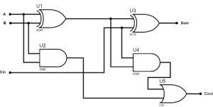
Fa = full adder, ha = half adder.
This results in low input capacitance and high speed operation. If a and b are the input bits . Half adder is a combinational arithmetic circuit that adds two numbers and produces a sum bit (s) and carry bit (c) as the output. Fa = full adder, ha = half adder. The output is the sum of the two bits (s) and the carry (c). In this video, i have explained cmos half adder with following timecodes: The schematic diagram of the cpl full adder circuit is shown in fig 4. The block diagram of a half adder is shown below. Half adder is a combinational circuit that performs simple addition of two single bit. Though the implementation of larger logic diagrams is possible with the above full adder logic a simpler symbol is mostly used to represent the operation. Digital circuit built from two logic gates. Fig.3 schematic diagram of existing half adder using static cmos technique. Draw the stick diagram of half adder circuit;
Appropriate device sizing can result in equal and symmetrical drive current which leads to a sunstainable design. Fa = full adder, ha = half adder. The output is the sum of the two bits (s) and the carry (c). Each full adder inputs a c . If a and b are the input bits .

Though the implementation of larger logic diagrams is possible with the above full adder logic a simpler symbol is mostly used to represent the operation.
Half adder is a combinational circuit that performs simple addition of two single bit. Draw the stick diagram of half adder circuit; Each full adder inputs a c . The circuit diagram of simplified half adder is shown in fig.6. Fa = full adder, ha = half adder. Appropriate device sizing can result in equal and symmetrical drive current which leads to a sunstainable design. In this video, i have explained cmos half adder with following timecodes: Gates implementation of half adder. Half adder is a combinational arithmetic circuit that adds two numbers and produces a sum bit (s) and carry bit (c) as the output. If a and b are the input bits . The output is the sum of the two bits (s) and the carry (c). Digital circuit built from two logic gates. This results in low input capacitance and high speed operation.
Cmos Diagram For Half Adder Circuit : Half Adder Circuit Theory And Working Truth Table Schematic Realization. The circuit diagram of simplified half adder is shown in fig.6. Each full adder inputs a c . Digital circuit built from two logic gates. The output is the sum of the two bits (s) and the carry (c). Though the implementation of larger logic diagrams is possible with the above full adder logic a simpler symbol is mostly used to represent the operation.


Comments
Post a Comment